EFX 2026 6–8 October, Messe Stuttgart: find us in hall 9, stand C29. Read the post →
Edge contacts

Gold Finger

Card-edge contacts that plug directly into a socket. Hard gold over nickel takes the mechanical wear that soft ENIG gold cannot, and the bevel is what lets the card find the socket without shaving the plating off on the first insertion.

At a glance
Plating Hard gold over Ni
Gold thickness 0.8 – 1.2 µm
Nickel underlay 3 – 6 µm
Bevel angle 15 – 60°
Bevel tolerance ± 5°

A gold finger is a plated contact at the board edge that mates directly with a socket — the classic example being a memory module or an add-in card. Unlike a soldered contact it has to survive mechanical wear, so the plating is hard gold: cobalt- or nickel-hardened, deposited over a nickel barrier, and considerably tougher than the thin soft gold of an ENIG finish.

Two things determine how long it lasts. The gold thickness sets the wear reserve — we plate 0.8 to 1.2 µm, towards the upper end where the card is inserted often. The bevel sets whether that reserve is consumed evenly or scraped off at one edge on the way in. A card-edge design that specifies the gold but not the bevel is only half specified.
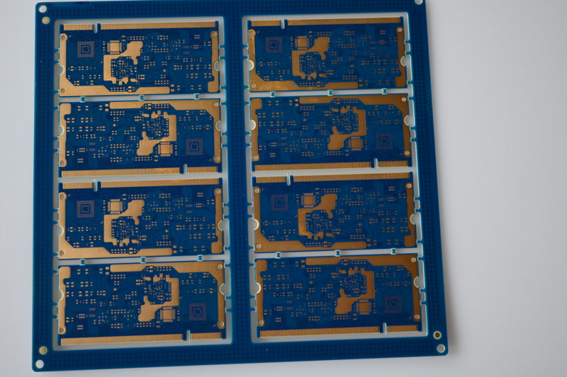
Gold Finger

What it delivers

[ Overview ]
01

Built for wear, not for solder

Hard gold over nickel is made for repeated insertion. ENIG gold is a fraction of a micron of soft gold and wears through quickly.

02

Bevelled for clean mating

A chamfer — 30° and 45° are the preferred angles within the 15 – 60° range — guides the card into the socket and stops the contact edge from ploughing the plating on insertion.

03

Selective plating

Only the contact area is hard-gold plated; the rest of the board keeps whatever finish suits assembly. You pay for gold where it does work.

Build and options

[ Datasheet ]
Feature Specification
Material FR-4, High-Tg FR-4, polyimide
Layers 1 – 6
Final thickness 0.5 – 2.0 mm
Copper 18 – 70 µm (standard 18 or 35 µm)
Contact plating Hard gold over nickel, Au 0.8 – 1.2 µm / Ni 3 – 6 µm
Bevel 15 – 60° (± 5°); 30° and 45° preferred
Surface finish ENIG on the board, hard gold on the contacts
Typical use Motherboards, PCIe and memory cards, network and storage gear

The usual build for this line. Anything outside it is normally still possible — ask and we will confirm.

Gold finger limits

[ Specification ]

Gold thickness follows the expected number of insertions. For frequently mated cards, specify the upper end of the range.

Parameter Standard Advanced Note
Gold thickness 0.8 µm 1.2 µm Hard gold, cobalt-hardened
Nickel underlay 3 – 5 µm 5 – 6 µm Barrier against copper diffusion
Bevel angle 30° / 45° 15 – 60° Tolerance ± 5°; measured from the board plane
Bevel depth ⅓ thickness to spec State it in the fabrication drawing
Bevel tolerance ± 5° ± 5° Across the whole angle range
Contact pitch ≥ 0.80 mm ≥ 0.635 mm Finer pitch needs tighter edge tolerance
Edge tolerance ± 0.15 mm ± 0.10 mm Routed edge to first contact
Keep-out to mask ≥ 0.30 mm ≥ 0.20 mm Solder resist must not reach the contact

Guide values for pre-selection. Binding values are confirmed per project against your data.

Typical applications

[ Use cases ]
Memory and expansion modules
Backplane plug-in cards
Industrial I/O cards with field replacement
Test adapters and probe interfaces
Instrumentation modules with hot-swap
Docking and cartridge interfaces

Design rules

[ Layout ]

The points below are what most often comes back as a query after data review. Settling them before layout freeze saves a loop.

01

Specify the bevel, not just the gold

Angle and depth belong in the fabrication drawing. A drawing that names 0.8 µm hard gold and says nothing about the chamfer leaves the most wear-relevant parameter to chance.

02

Keep solder resist off the contacts

Allow at least 0.3 mm between the resist edge and the plated contact. Resist creeping onto a finger interferes with the socket and can flake into it.

03

Mind the edge tolerance

Contact position is measured from the routed edge, so routing tolerance adds directly to contact misalignment. On fine pitches this is the binding constraint, not the plating.

04

Do not run gold fingers to a scored edge

V-scoring leaves a rough, uneven edge that will not bevel cleanly. Card edges carrying contacts must be routed, not scored.

Frequently asked

[ FAQ ]
Why not just use ENIG on the contacts?

ENIG puts down 0.025 – 0.075 µm of soft gold, intended for solderability rather than wear. It will survive a handful of insertions and then expose the nickel. For anything repeatedly mated you need hard gold at 0.8 µm or above.

Can I combine gold fingers with another finish?

Yes, and it is normal. The contacts get selective hard gold, the rest of the board gets ENIG, immersion tin or whatever suits your assembly. Say so in the drawing so both are tooled.

How much does the bevel cost?

It is a separate mechanical operation, so it adds a fixed setup and a small per-part cost. On any card actually intended for repeated insertion it is not optional.

Do gold fingers need to be on both sides?

Only if the socket contacts both sides — most edge sockets do. Check the connector datasheet; single-sided contact does exist and halves the plating area.

Related

[ Cross-reference ]

Does this fit your project?

Send us your data or a rough sketch. We check feasibility, name the cost drivers and answer within one working day.