The capability extract shows in thirty seconds what runs as standard and what carries a surcharge.
See capabilities →Send the files and an engineer reviews them against your build — free, before you enquire.
To the data check →The workhorse of the portfolio. Four to over forty layers, FR-4 or High-Tg, with registration held tightly enough that a 24-layer build still lands within the annular ring. Most of the engineering happens in the stack-up, not in the routing.
A multilayer board is a stack of thin cores and prepreg pressed into one piece. Everything that later determines whether it works — impedance, warpage, drill registration, thermal behaviour — is decided by how that stack is put together, long before the first track is routed.
The two questions that come back most often after data review are both structural. Is the build symmetrical around the centre, and does the copper distribution balance across the panel? An asymmetric or copper-starved build warps during the lamination cycle, and a board that warps by more than about 0.75 % will not place reliably on a modern SMT line.
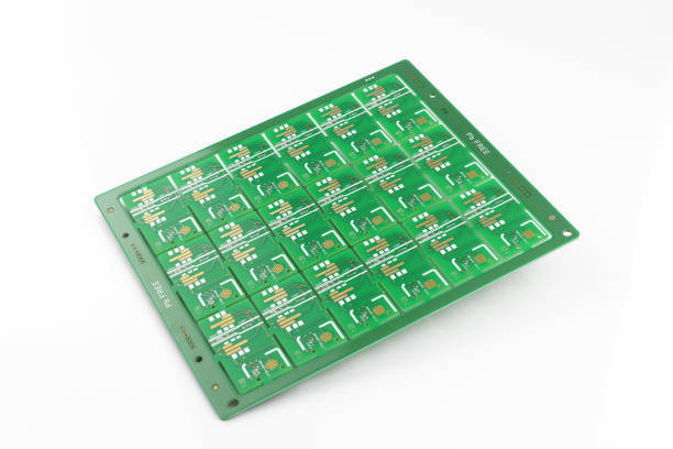
Four to over forty layers in one process family. A design can grow a layer pair late without changing supplier or qualification.
Layer-to-layer registration held to ± 75 µm, so annular rings survive even in thick builds with many drill cycles.
The best-understood line in the portfolio. Quantity, layer count and copper weight determine the price almost linearly — which makes it easy to budget.
| Feature | Specification |
|---|---|
| Material | FR-4, High-Tg FR-4, halogen-free, polyimide and mixed builds |
| Layers | 4 – 40+ |
| Final thickness | 0.5 – 4.0 mm |
| Copper | 12 – 105 µm (standard 18 or 35 µm) |
| Surface finish | ENIG, OSP, immersion silver/tin, lead-free HASL |
| Solder mask | Green, blue, black, white |
| Typical use | Telecommunications, automotive, medical, industrial control |
The usual build for this line. Anything outside it is normally still possible — ask and we will confirm.
Standard values run without surcharge across the plant network. The advanced column is available but should be confirmed against your data before layout freeze.
| Parameter | Standard | Advanced | Note |
|---|---|---|---|
| Layer count | 4 – 16 | 18 – 40+ | Above 24 layers expect a longer lamination sequence |
| Line / gap | 100 / 100 µm | 75 / 75 µm | Inner layers with heavy copper need more |
| Final thickness | 0.8 – 3.2 mm | 0.4 – 6.0 mm | Thin and very thick builds both need handling care |
| Copper weight | 18 / 35 µm | 70 / 105 µm | Heavier copper widens the required track and gap |
| Min. drill Ø | 0.25 mm | 0.20 mm | Mechanical; below that see the microvia figures |
| Aspect ratio | 8 : 1 | up to 16 : 1 | 14 : 1 at Ø 0.20 mm, 16 : 1 at Ø 0.25 mm |
| Registration | ± 100 µm | ± 75 µm | Layer to layer, across the panel |
| Warpage | ≤ 0.75 % | ≤ 0.50 % | To IPC-A-600; needs a symmetrical build |
Guide values for pre-selection. Binding values are confirmed per project against your data.
The points below are what most often comes back as a query after data review. Settling them before layout freeze saves a loop.
Mirror the stack around the centre: same core thickness, same copper weight, same prepreg at equal distance from the middle. An asymmetric build warps during the press cycle, and no amount of flattening afterwards fixes it properly.
Large empty areas on one layer and dense copper on the next make resin flow unevenly. Add copper thieving in unused areas — it costs nothing and measurably improves thickness consistency.
Every additional drill and press sequence adds days of lead time and a step in price. Decide how many sequences the design needs at stack-up stage, not when the buried vias appear in routing.
The standard is ≥ 125 µm. If your design lives closer to the limit, say so — we can tighten registration in production, but only if it is specified before tooling.
Series production runs comfortably to 24 layers. Beyond that, up to and past 40 layers is feasible but needs a feasibility review — lamination sequence, aspect ratio and registration all tighten at once, and lead time grows.
From roughly eight layers upward, or with more than two lead-free solder cycles, High-Tg is the safer choice. The surcharge is around 10 – 20 %, which is small against the cost of delamination found at assembly.
Almost always build-up asymmetry or uneven copper distribution. Both are fixed in the stack-up, not in production. Send us the intended stack and we will flag it before tooling.
Yes, and it is common — 35 µm on signal layers with 70 µm on a power plane, for example. Remember that the heavier layer needs wider tracks and gaps, so the routing constraints differ per layer.
Send us your data or a rough sketch. We check feasibility, name the cost drivers and answer within one working day.