The capability extract shows in thirty seconds what runs as standard and what carries a surcharge.
See capabilities →Send the files and an engineer reviews them against your build — free, before you enquire.
To the data check →Above a few hundred megahertz a track stops being a wire and starts being a transmission line. Holding its characteristic impedance to a stated tolerance is what keeps the eye open — and the test coupon in the panel is what proves it was held.
Characteristic impedance is set by four things: track width, dielectric thickness to the reference plane, the dielectric constant of the material, and the copper thickness. Three of them are ours; the first one is yours. Which is why an impedance-controlled job is always a conversation about the stack-up before it is a production order.
What we do in practice is take your target impedance and layer assignment and calculate the stack-up backwards — adjusting dielectric thicknesses and, where necessary, proposing a corrected track width. You get the calculated stack back for approval before tooling. A design routed to a guessed width and then declared impedance-controlled is the single most common source of failed first articles.
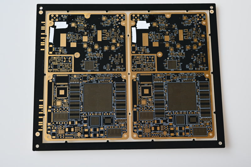
We work back from your target impedance to a real build using the actual laminate data, and send it for approval before tooling starts.
A TDR coupon rides in the panel and is measured per production lot. The result is the documentary evidence if performance is ever questioned.
± 10 % is the published tolerance and covers most digital work without a surcharge. Tighter requirements are subject to a technical review of the stack-up.
| Feature | Specification |
|---|---|
| Material | FR-4, Rogers, PTFE, Arlon, Taconic |
| Layers | 2 – 20+ (set by frequency and design) |
| Final thickness | 0.2 – 3.0 mm |
| Copper | 12 – 105 µm (standard 18 or 35 µm) |
| Solder mask | Thin mask, tuned for minimal reflection |
| Tolerance | ± 10 %; tighter subject to technical review |
| Surface finish | ENIG, OSP, immersion silver/tin, lead-free HASL |
| Typical use | High-frequency comms, 5G, high-speed data, radar, networking |
The usual build for this line. Anything outside it is normally still possible — ask and we will confirm.
The tolerance you specify drives both the stack-up effort and the price. The published tolerance is ± 10 %; anything tighter is subject to a technical review before it is confirmed.
| Parameter | Standard | Advanced | Note |
|---|---|---|---|
| Single-ended | 50 Ω | 40 – 120 Ω | Other targets on request |
| Differential | 90 / 100 Ω | 85 – 120 Ω | USB, Ethernet, LVDS, PCIe |
| Tolerance | ± 10 % | on review | Tighter tolerances are subject to technical review |
| Reference plane | adjacent | dual | Every controlled layer needs a solid reference |
| Test coupon | per panel | per panel | TDR measured, report supplied on request |
| Frequency range | ≤ 5 GHz | ≤ 20 GHz | Above this see High Frequency materials |
| Etch compensation | applied | applied | We adjust the artwork; do not pre-compensate |
| Material | FR-4 / High-Tg | Low-loss / RF | Dk stability matters more as frequency rises |
Guide values for pre-selection. Binding values are confirmed per project against your data.
The points below are what most often comes back as a query after data review. Settling them before layout freeze saves a loop.
A controlled track that crosses a split or a gap in its reference plane loses its impedance at that point regardless of what the stack-up says. Route the plane first, then the signal.
We apply etch compensation in production. If you have already widened the tracks for it, the compensation is applied twice and the impedance comes out low.
The coupon needs space in the panel border. In a series panel this costs nothing; in a tightly nested prototype panel it can cost a copy of the board — tell us early.
Impedance requirements written only in the schematic or an email do not reach production. Put target, tolerance and the layers concerned in the fabrication drawing.
At ± 10 % on a standard stack-up, usually very little — the work is in the calculation and the coupon measurement. Anything tighter constrains etch and dielectric tolerance across the whole panel, so it is subject to a technical review and priced per design.
Yes, and we prefer to. Send the target impedances, the layer assignment and the layer count; we send back a calculated build with track widths for approval before tooling.
The lot is held. Because the coupon is measured per panel, the deviation is caught in production rather than in your assembly line — which is the whole point of the coupon.
Generally not, unless the trace is long relative to the signal edge rate. It is the edge rate rather than the clock frequency that matters — a slow clock with a 200 ps edge behaves like a fast one.
Send us your data or a rough sketch. We check feasibility, name the cost drivers and answer within one working day.